
Transistorized Gating Circuit (1961)
U.S. Patent No. 2,972,726, granted on May 2, 1961, to Philip Emile, Jr., describes a high-precision electronic “gate” designed for the U.S. Army. In the early days of transistor technology, electronic gates—circuits that allow or block a signal based on a control pulse—often suffered from distortion or a “pedestal” effect (an unwanted shift in the DC voltage level when the gate opened or closed).
Emile’s invention solved these issues by using a unique “T-network” of resistors and taking advantage of the physics of a saturated transistor, creating a circuit that could pass signals cleanly without shifting the background voltage.
The Anatomy of the Gate
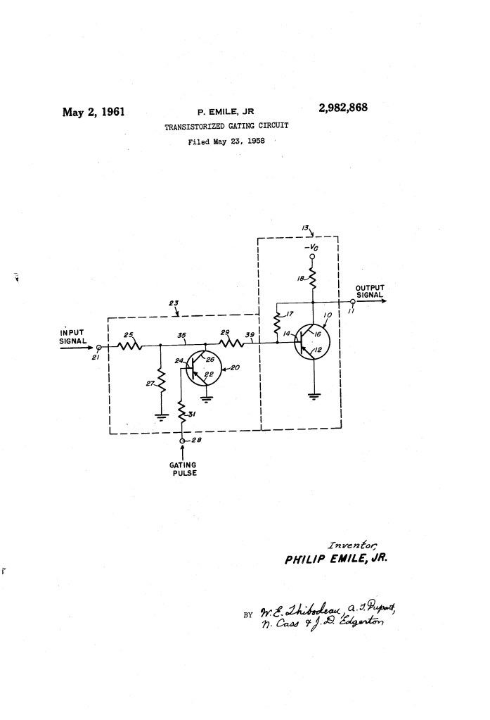
The circuit is divided into two functional blocks: the Input Circuit (23) and the Amplifier (13).
1. The T-Network and Switching Transistor
The heart of the invention is a T-shaped arrangement of three resistors (25, 27, and 29). A switching transistor (20) is placed in parallel with the middle resistor (27).
- The “Closed” State (Gated): When a negative gating pulse is applied to the base of the switching transistor, it becomes saturated.
- Saturation Physics: Emile explains that a saturated transistor acts as a near-perfect short circuit (less than 10 ohms) for both positive and negative signals.
- Signal Blocking: Because the transistor shorts the middle of the “T” to ground, the input signal is shunted away, preventing it from reaching the amplifier.
2. The Common Emitter Amplifier
Any signal that survives the gate is sent to a PNP transistor (10) configured as a common emitter amplifier. This stage is biased for Class A operation, meaning it is always “on” and ready to amplify the incoming signal with minimum distortion.
Overcoming the “Gating Pedestal”
A major problem in 1950s gating circuits was that the gating pulse itself would leak into the output, causing the DC level to “jump” up or down. Emile’s T-network is specifically designed to prevent this:
- Impedance Matching: By carefully choosing the values of resistors 27 and 29, the circuit ensures that the impedance “seen” by the amplifier remains relatively constant whether the gate is open or closed.
- The Result: The DC level at the output only shifts by about 0.5 volts, a negligible amount compared to the signal strength. This allows for DC coupling without the need for capacitors, which often cause signal distortion.
Performance Specs
In the specific embodiment described in the patent, the circuit achieved the following:
| Component | Value / Result |
| Input Signal | 10V peak-to-peak |
| Amplified Output | 7.5V peak-to-peak |
| Overall Gain | 0.75 |
| Saturated Impedance | < 10 Ohms |
| DC Level Shift | ~0.5 Volts |
Key Applications
Because this circuit passes signals without distortion and manages DC levels so precisely, Emile noted it could be used for:
- Phase Comparison: Measuring the timing difference between two signals.
- Pulse/Amplitude Modulation: Using the gating pulse to “shape” the input signal into data pulses.
- Sample Gating: Taking quick “snapshots” of a continuous signal for processing.
Technical Summary
The patent claims a gating circuit comprising a one-stage common emitter amplifier fed by a three-resistor T-network. The use of a switching transistor in parallel with the middle resistor allows the circuit to function as a high-speed, low-distortion switch that is uniquely effective at minimizing DC pedestal shifts.
