
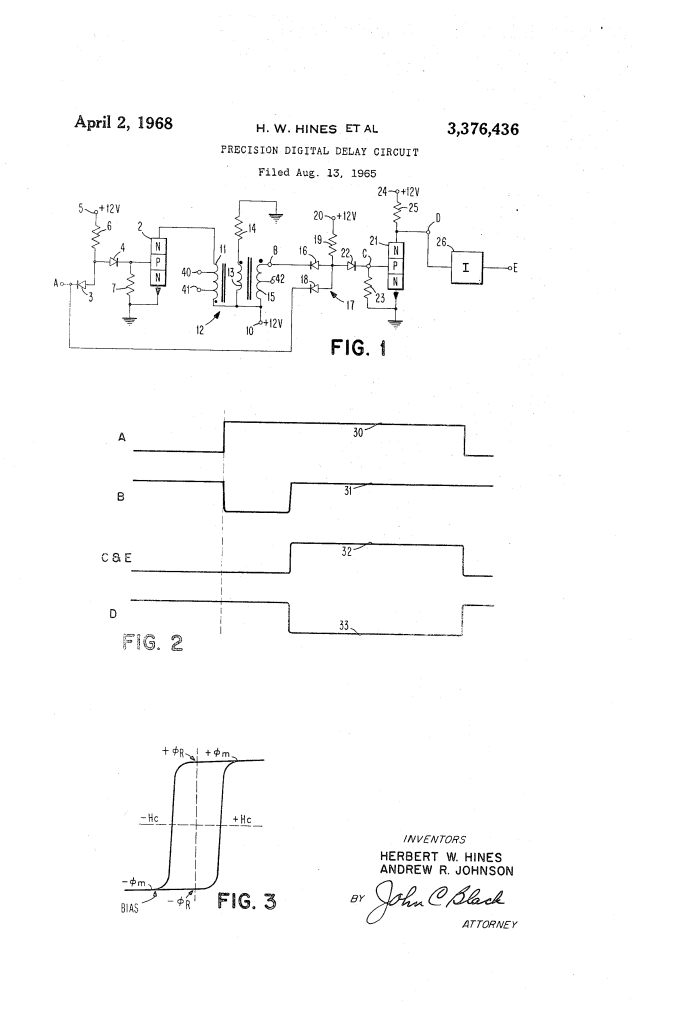
Precision Digital Delay Circuit (1968)
U.S. Patent No. 3,376,436, granted on April 2, 1968, to Herbert W. Hines and Andrew R. Johnson, describes an ultra-precise digital delay network designed to eliminate timing jitter and thermal drift in high-speed digital computing systems. Herbert Hines and Andrew Johnson, engineers based in Endwell, New York, assigned the patent to the International Business Machines Corporation (IBM) in Armonk, New York.
This specific invention solved a persistent obstacle in digital logic design: conventional electronic delay circuits relied on resistor-capacitor (RC) or resistor-inductor (RL) timing networks and individual transistor switching parameters. In mass production, component manufacturing tolerances and ambient temperature swings caused substantial variations in delay times, introducing signal skew, pulse distortion, and timing errors across complex computer systems. Hines and Johnson developed a circuit where the delay is dictated by the stable, physical magnetic saturation properties of a square-loop transformer core rather than temperature-sensitive components.
The Innovation: The Square-Loop Magnetic Inhibit Gate
The core breakthrough lies in coupling a logical AND gate with a transformer built around a magnetic core possessing a square-loop hysteresis characteristic. Rather than relying on an analog charge curve, the circuit uses the fixed switching time required to drive the transformer’s magnetic core from negative magnetic saturation to positive magnetic saturation.
- The Dual-Input Logical AND Circuit (17)The incoming bivalued digital pulse is split. One branch feeds directly into one input (diode 18) of the logical AND gate. The other branch drives the base of a high-speed transistor switch (2).
- Magnetic Core Inhibit Action (11, 12, 15)The transistor switch drives current through the transformer primary winding (11). As long as the core is actively swinging between its negative and positive saturation levels, the secondary winding (15) generates a negative-going inhibit pulse at node B. This negative signal clamps the second input of the AND gate (diode 16), holding the AND gate OFF.
- Saturation and Output ReleaseThe instant the magnetic core completes its swing and enters positive saturation, the induced voltage in the secondary winding collapses, the inhibit pulse at B snaps positive, and the AND condition is satisfied. The delayed digital pulse immediately passes to the output inverters (21, 26).
Why the Square-Loop Transformer?
- Immunity to Temperature: In a typical tape-wound square-loop core, total flux change varies by only 2.4% over an operating range from -10°C to +50°C.
- Freedom from Transistor Variations: The inhibit pulse reaches its clamping level in roughly 50 nanoseconds, making the timing essentially independent of the turn-on speed or beta tolerances of the driving transistor.
- Eliminates Skew: Because the core’s saturation properties are fixed by design, mass-produced circuits exhibit virtually identical delay intervals without pulse width distortion.
Key Circuit Components
The apparatus combines passive magnetic switching with solid-state digital logic:
| Component | Schematic Callout | Function in Circuit |
| Transistor Switch | 2 | Common-emitter NPN switch that drives current into the primary winding when an input pulse arrives. |
| Input Steering Network | Diodes 3, 4; Resistors 6, 7 | Biasing and coupling diodes that turn on transistor 2 upon receiving a positive input transition as low as 0.5 V. |
| Square-Loop Transformer | 12 | Core possessing a sharp square-loop hysteresis curve and low coercive force; sets the physical delay interval. |
| Primary Winding | 11 (with taps 40, 41) | Magnetizing coil; selecting different taps alters primary turn count (N) to adjust delay duration. |
| Bias Winding | 13 (with resistor 14) | Continuously energized winding that resets the core to negative saturation when no input signal is present. |
| Secondary Winding | 15 (with taps 42) | Generates the negative-going inhibit pulse at terminal B while the magnetic flux transitions across the loop. |
| Logical AND Gate | 17 (Diodes 16, 18; Resistor 19) | Inhibits pulse output until the secondary winding signal collapses upon full core saturation. |
| Inverter Stages | Transistors 21, 26; Resistors 23, 25 | Restores digital signal levels; provides inverted output at node D and non-inverted delayed output at terminal E. |
How the Circuit Functions
The delay circuit executes a precise five-step sequence for every incoming digital pulse:
| Step | Action | Operational Purpose |
| 1. Signal Arrival | Positive-going pulse 30 arrives at input terminal A, splitting to diode 18 and the base of switch 2. | Arms one side of AND gate 17 and initiates rapid turn-on of transistor 2. |
| 2. Core Transition | Switch 2 conducts, routing collector current through primary winding 11 to flip the magnetic core toward positive saturation. | Begins the core’s flux transition from minus-phi-m to plus-phi-m. |
| 3. Inhibit Gating | Secondary winding 15 develops a negative inhibit voltage 31 at node B within 50 nanoseconds, reverse-biasing diode 16. | Blocks AND circuit 17 from triggering, preventing premature output spikes or transients. |
| 4. AND Satisfaction | Core reaches maximum positive flux saturation; the induced voltage at B rapidly collapses and rises to supply rail 10. | Satisfies the AND condition; node C turns on inverter 21 to produce delayed pulse output 32. |
| 5. Core Reset | Input pulse 30 terminates; switch 2 turns off and bias winding 13 restores core flux to negative saturation. | Resets the magnetic core to initial state, ready for the next incoming pulse. |
Performance: Precision Delay Metrics
The total signal delay corresponds directly to the core’s magnetic switching time (t), governed by the equation:
t = (N * delta-phi) / E
Where:
- N is the number of primary turns.
- delta-phi is the total flux change between negative and positive saturation (2 * phi-m).
- E is the transistor supply voltage at terminal 10.
Operational Test Values (Tape-Wound Core):
- Primary Turns (N): 10 turns.
- Total Flux Change (delta-phi): 240 x 10^-8 lines.
- Supply Voltage (E): 12 volts.
- Nominal Delay Achieved: Exactly 2.0 microseconds.
- Maximum Delay Variation (Delta-t): Over an operating span of -10°C to +50°C and a supply voltage variation of plus-or-minus 0.5 V, total delay fluctuation remained within 0.06 microseconds.
About the Inventors and IBM
The patent represents a collaborative achievement by engineers at IBM’s facilities in Endwell and Endicott, New York:
- Herbert W. Hines and Andrew R. Johnson: Industrial electrical engineers specializing in solid-state circuit design, digital memory interfacing, and magnetic-core timing systems during the buildout of second- and third-generation computing platforms.
- Computing Impact: In systems like the IBM System/360 era, synchronizing data words across arithmetic logic units and memory buses demanded microsecond-scale delay lines with low skew. Hines and Johnson provided a low-cost, easily packaged solution that decoupled clock timing from transistor tolerances and ambient room temperatures.
Summary of Claims
The patent explicitly claims:
- A digital delay circuit comprising a logical AND gate with two inputs, an electronic switch activated by an input pulse, and a square-loop hysteresis transformer having primary, secondary, and bias windings.
- Using the transformer secondary winding to apply an inhibit pulse to the second input of the AND gate strictly during core flux switching from negative to positive saturation, blocking output until switching completes.
- Restoring the magnetic core to its initial negative saturation level via an active bias winding whenever the input pulse terminates.
- Incorporating taps on the transformer primary winding to allow user-selectable, discrete delay durations.
