
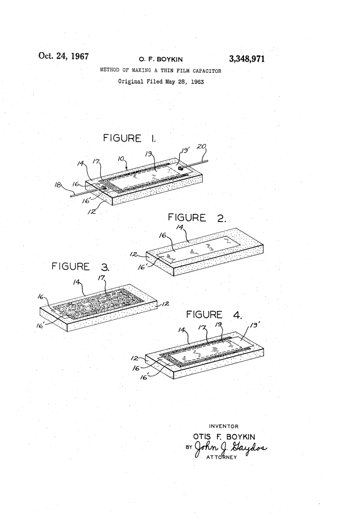
Method of Making a Thin Film Capacitor (1967)
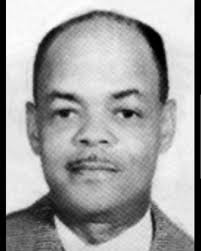
U.S. Patent No. 3,348,971, granted on October 24, 1967, to Otis F. Boykin (assigned to CTS Corporation), describes an innovative method for manufacturing thin-film micro-capacitors designed for printed circuits. Otis Boykin, an inventive electronics engineer based in Chicago, Illinois, pioneered micro-components that revolutionized consumer electronics, aerospace guidance, and life-saving medical devices.
This specific invention solved a persistent bottleneck in early printed circuitry: how to produce high-yield, compact capacitors capable of operating at high working voltages and frequencies without relying on fragile ceramic discs or costly, low-yield vacuum deposition and anodization systems.
The Innovation: The Liquid Organometallic Dielectric
Prior thin-film capacitors suffered from extreme production hurdles. Ceramic disc models required high firing temperatures (around 2500°F) that eliminated high-conductivity metals like gold. Vacuum-deposited alternatives relied on surface anodization, which limited dielectric thickness, drove dissipation factors to a poor 5%, and caused frequent voltage breakdowns.
Boykin bypassed vacuum chambers and extreme kiln heat entirely. His breakthrough was formulating an all-liquid admixture of organic metal solutions (resinates) combined with glass-forming organo compounds. When screen-printed and fired in air below 800°C, the liquid metal compounds decompose at a molecular scale into high-k dielectric oxides (such as barium titanate or lead tantalate) while the glass matrix simultaneously fuses, encasing the dielectric particles and bonding them securely to the underlying electrode.
Why Liquid Organometallic Precursors?
- Molecular Dispersion: Metal resinates mix uniformly in liquid phase, ensuring defect-free dielectric films without granular clumping.
- Low-Temperature Firing: Curing below 800°C permits the use of superior, low-resistance noble metal electrodes like gold rather than refractory platinum.
- Controlled Thickness: Layering the liquid dielectric avoids self-limiting anodization, enabling high dielectric strength and breakdown ratings exceeding 500 volts DC.
- Ultra-Low Dissipation: Sintered oxide-glass composites lower the dissipation factor to less than 0.25%, sharply increasing operating efficiency (Q factor).
Key Chemical and Material Components
The thin-film capacitor uses a multi-layered composite structure where each layer serves a specific electrical and mechanical purpose:
| Component | Chemical Formulation | Function in Capacitor |
| First Electrode (16) | Liquid gold resinate and powdered glass frit (~50,000 Å thick) | Bottom conductive electrode; bonds directly to the ceramic substrate (12) upon firing below 800°C. |
| Dielectric Precursor Matrix (17) | Transition metal resinates (Ta, Ti, Zr, Nb, Hf, or W) | Pyrolyzes into active, high-permittivity dielectric oxide crystals (e.g., tantalum pentoxide or titanium dioxide). |
| Modifier Resinates | Ba, Ca, Sr, Cu, Ni, Pb, or Zn resinates | Reacts with dielectric oxides during firing to synthesize tailored titanates or tantalates for temperature and frequency stability. |
| Vitreous Binder Matrix | Lead, boron, and silicon resinates / organosols | Decomposes into a pyrolyzed borosilicate glass that molecularly bonds the dielectric particles to each other and to the electrode. |
| Second Electrode (19) | Noble metal resinate (preferably gold) in glass matrix | Top conductive plate; covers the active dielectric area and extends to contact pad 19′ on substrate 12. |
| Substrate (12) | High-purity alumina ceramic | High-temperature electrically insulating base providing structural support for the micro-circuitry. |
How the Apparatus Functions
Fabricating the capacitor follows a sequenced screen-and-fire cycle that builds up the active layers directly on the ceramic base:
| Step | Action | Operational Purpose |
| 1. Base Deposition | Screen-print liquid gold resinate and powdered glass slurry onto substrate 12. | Establishes bottom conductive electrode 16 and terminal contact 18. |
| 2. Base Firing | Fire the substrate below 800°C in an oxidizing atmosphere. | Burns off organic screening agents and fuses the glass-gold matrix to top surface 14. |
| 3. Dielectric Application | Screen-print the liquid resinate blend (transition metal, modifier, and glass resinates) over electrode 16. | Spreads the dielectric precursor film 17 across the active capacitive area while leaving terminal 16′ exposed. |
| 4. Dielectric Pyrolysis | Fire the assembly below 800°C in an oxidizing atmosphere. | Volatilizes organic resinates, oxidizes metals into microcrystalline dielectrics, and fuses the glass matrix. |
| 5. Successive Layering | Repeat screen-and-fire steps for dielectric film 17 (optional). | Eliminates pinholes and surface flaws, lifting breakdown voltage beyond 500 V DC. |
| 6. Counter-Electrode Finish | Screen-print and fire top gold electrode layer 19 over dielectric 17. | Completes the capacitor structure, routing terminal contact 19′ down to surface 14. |
Tailored Dielectric Formulations
Boykin demonstrated that altering the liquid resinate blend directly tunes the capacitor’s operating properties:
- Lead Zinc Tantalate (Example I): Combining tantalum resinate, lead resinate, and zinc resinate yields zinc lead tantalate embedded in borosilicate glass, substantially raising the dielectric constant (K factor).
- Calcium Barium Titanate (Example III): Admixing titanium, barium, and calcium resinates forms calcium barium titanate, delivering an exceptionally stable temperature coefficient.
- Strontium Titanate (Example IV): Synthesizing strontium titanate in the glass layer creates a flat, straight-line capacity response across wide radio-frequency ranges.
About the Inventor: Otis F. Boykin
Otis Frank Boykin was an acclaimed African American inventor and electronics engineer whose component designs helped define the microelectronics era:
- Life-Saving Technology: Boykin developed precision wire-type and cermet resistors along with capacitor architectures that enabled compact, radiation-resistant, and high-reliability circuitry. A modified version of his control circuit became the cornerstone of the modern implantable cardiac pacemaker.
- Aerospace and Defense: His resilient electrical components were incorporated into guided missile tracking systems, military aircraft controls, and early IBM mainframe computing mainframes.
- Prolific Legacy: Over his career, Boykin earned more than 25 patents across electrical components, consumer technologies, and air filtration systems.
Summary of Claims
The patent explicitly claims:
- A method of manufacturing a thin-film capacitor by applying and bonding a noble metal electrode (non-oxidizable below 800°C) to an insulating base, applying a thin layer of glass particles or glass-forming resinates admixed with an oxidizable metal resinate, firing in an oxidizing atmosphere below 800°C, and applying a top noble metal electrode.
- Synthesizing the dielectric layer from transition metal compounds selected from tantalum, zirconium, niobium, aluminum, titanium, hafnium, and tungsten.
- Reacting the primary dielectric metal with secondary modifier resinates (barium, calcium, strontium, copper, nickel, lead, or tin) to formulate complex compounds such as barium titanate.
- A high-voltage capacitor architecture built on a permanent heat-resistant support capable of withstanding breakdown potentials exceeding 500 volts DC.
