
Electrical Resistance Element and Method of Making the Same (1967)
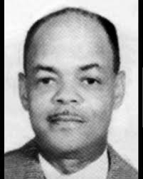
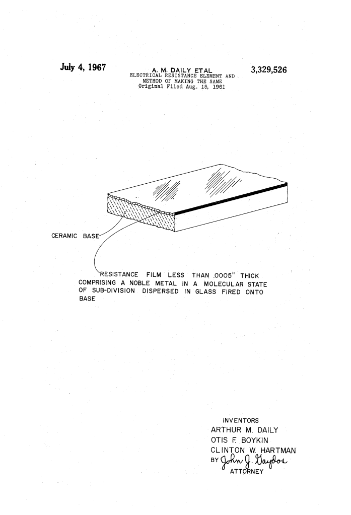
U.S. Patent No. 3,329,526, granted on July 4, 1967, to Arthur M. Daily, Otis F. Boykin, and Clinton W. Hartman (assigned to CTS Corporation), details a breakthrough method for manufacturing ultra-thin, high-precision ceramic-metal (cermet) resistors. Otis Boykin, an inventive electronics pioneer who developed foundational components for guided missiles, computers, and medical devices, collaborated with CTS Corporation engineers to solve a key manufacturing barrier during the early aerospace and miniaturization boom.
As guidance systems for rockets and missiles became smaller, variable resistance controls (trimmers and potentiometers) shrank to fractions of an inch. Because an element’s physical area dictates its available “squares” of resistance, compact controls were physically limited to approximately twenty squares. Generating high overall resistances—from 5,000 ohms up to 8 megohms—demanded resistance densities between 50,000 and 400,000 ohms per square. Conventional thick-film methods (films of .0005 to .003 inch) could not consistently hit these high resistance targets without severe tolerances drifting, structural bubbling, or electrical failure.
The Innovation: Acicular Ruthenium in Micro-Layered Glass
Daily, Boykin, and Hartman broke with prevailing industry practices, which assumed films needed to be thick to remain stable. Instead, they discovered that total film thickness had to remain well below .0005 inch (typically between .00003 and .00021 inch), built up through successive, individually fired micro-layers where no single layer exceeds .00005 inch.
To achieve unmatched resistance densities, they introduced ruthenium in an organic solution (organosol) rather than relying on standard noble metals like gold, silver, or platinum.
Why Ruthenium?
- Acicular Needle Structure: Unlike most noble metals, which possess a face-centered cubic structure that grows into granular, low-resistance clumps, ruthenium exhibits a hexagonal close-packed crystal structure. It precipitates out in long, needle-like (acicular) crystals less than 2 microns in size (mostly sub-micron).
- High Aspect-Ratio Pathways: These interlocking microscopic needles create an unbroken conductive path with an exceptionally high ratio of length to cross-sectional area, yielding high electrical resistance without breaking conductivity.
- Precise Tolerance Control: Applying extremely low concentrations (0.5% to 13% by weight, optimally around 2%) dispersed in a glass matrix enables repeatable production in the 50,000 to 400,000 ohms per square range.
Key Chemical and Material Components
The composition is formulated from an organometallic precursor slurry designed for silk screening:
| Component | Weight in Unfired Mixture | Function in Resistance Element |
| Ground Glass Frit | 4% to 9% (8.70% in Example) | Finely ground lead borosilicate glass (under 325 mesh) that melts into the dielectric carrier matrix and fuses to the substrate. |
| Ruthenium Organosol | 4.35% (yielding 0.04% to 0.64% Ru) | Metal resinate, glycinate, or naphthenate dissolved in oil that thermally decomposes into acicular metallic ruthenium crystals. |
| Screening & Viscosifying Agent | 86.95% to 96% | Ethylcellulose dissolved in trichloroethylene-fenchone; suspends the glass powder during silk-screening and burns off cleanly during firing. |
| Ceramic Substrate | Solid base | High-temperature non-conductive ceramic (lapped and polished) that bonds with the corrosive lead borosilicate glaze at 800 C. |
Performance: Conquering the High-Resistance Range
The multi-layer technique eliminated “blowing” (blistering caused by trapped organic gases escaping through thick molten glass) and bypassed thermal expansion mismatches between the ceramic base and glass glaze.
Production Test Run on Miniature Units (Target: 5 Megohms Total Resistance):
- Target Resistance Density: ~385,000 ohms per square across a 13-square miniature element.
- First Fired Layer: Provided planarization, often reading infinite resistance as the molten glass settled into microscopic surface cavities.
- Three Fired Layers (.00009 inch total thickness): 36 out of 50 units reached the required 5 megohms within strict operational tolerances.
- Four Fired Layers (.00012 inch total thickness): 12 additional units hit the 5 megohm target.
- Yield Efficiency: 48 out of 50 units (96%) achieved exact high-range specifications, a precision benchmark previously unattainable in mass production.
The Manufacturing Process
The inventors established a three-stage heating profile completed in under 30 minutes:
- Surface Preparation: Lap and polish the ceramic substrate to eliminate surface pits and micro-imperfections.
- Formulate Slurry: Blend ground glass frit (under 325 mesh) with ruthenium organosol, mill thoroughly, and incorporate the ethylcellulose screening and viscosifying vehicle.
- Screen Printing: Silk-screen a pattern layer between .001 and .003 inch thick (containing roughly 2% glass by volume).
- Stage 1 Burn-Off (150 C for 10 minutes): Volatilizes solvent carriers and liquid screening agents.
- Stage 2 Organosol Reduction (350 C for 10 minutes): Initiates chemical breakdown of the metal resinate and burns away carbon residues.
- Stage 3 Glaze Fusion (800 C for 5 minutes): Melts the lead borosilicate glass frit, fully reduces the ruthenium into minute needle crystals, and bonds the layer to the ceramic.
- Stepwise Verification: Cool in air, measure electrical resistance, and repeat steps 3 through 6 (typically 2 to 4 cycles) until the target resistance value is achieved.
About the Inventor: Otis F. Boykin
Otis Frank Boykin was an African American inventor and electrical engineer whose precision resistor innovations transformed mid-century electronics:
- Defense and Aerospace: Boykin’s wire-type and cermet resistor designs dramatically reduced electronic manufacturing costs while withstanding extreme temperature swings, accelerations, and radiation inside military aircraft, guided missiles, and spacecraft.
- Medical Milestones: His micro-resistor circuitry enabled the control unit used in the modern implantable cardiac pacemaker, providing the reliable component longevity needed to maintain life-saving cardiac rhythms.
- Prolific Inventor: Boykin held over 25 patents across variable resistors, capacitor units, electrical resistance matrices, and electronic air-cleaning systems before his death in 1982.
Summary of Claims
The patent explicitly claims:
- An electrical resistance element comprising a ceramic base supporting a ruthenium-containing glass film less than .0002 inch thick, where the ruthenium has a hexagonal close-packed crystalline structure and acicular growth.
- A cermet resistance element with a sheet resistivity between 50,000 and 400,000 ohms per square, comprising 87% to 99.5% by weight glass and 0.5% to 13% by weight dispersed ruthenium.
- An unfired screen-printable composition consisting of 4% to 9% ground glass frit, 0.04% to 0.64% dissolved organometallic ruthenium, and 91% to 96% organic screening agent.
- A multi-step firing method featuring sequential heating at approximately 150 C, 350 C, and 800 C for total cycles under one hour, repeating layer applications until the predetermined resistance value is achieved.
