

Electrical Capacitor and Method of Making the Same, Otis F. Boykin, Patent No. 3,191,108
The patent by Otis F. Boykin of Chicago, Illinois, describes an electrical capacitor and method of making the same. This invention is a micro-miniature, high-capacity solid-state component—connotatively designated as a “dot capacitor”—engineered specifically for high-density, modular electronic integration such as the “Swiss Cheese” or breadboard packaging architectures of the mid-20th century. By executing a controlled, in-situ chemical conversion of the surface of a refractory metal body (such as tantalum or titanium) into a dual-phase ceramic dielectric layer consisting of native metal oxides integrated with perovskite-structured lead tantalate or lead titanate, Boykin eliminated the structural fragility and volumetric inefficiencies of contemporary capacitors. This process allowed for consistently reproducible electrical profiles, low dissipation factors, and exceptional thermal stability in ultra-small packages.
The “Why” (The Microelectronic Pain Point)
During the rapid shift toward advanced electronic packaging concepts in the mid-20th century, the electronics industry faced a critical physical bottleneck: the need for high-capacitance components that occupied minimal physical volume while maintaining high dielectric breakdown thresholds and low dissipation (Q) factors. Contemporary micro-capacitors struggled with process-induced failures. If an independent ceramic dielectric material was fabricated separately and bonded to an electrode, the resulting component was bulky and prone to mechanical delamination.
Conversely, attempting to completely convert a metal substrate into a pure dielectric compound destroyed the molecular bond between the active dielectric layer and the underlying conductive core, causing the component to disintegrate under minor handling or vibrational stress. Engineers required a highly precise, scalable manufacturing methodology that could synthesize a robust, multi-layered dielectric matrix in situ directly on a micro-pellet electrode without compromising structural adhesion or electrical performance.
Inventor Section: Engineering Philosophy
Otis F. Boykin was a visionary African American electronics engineer and inventor whose contributions fundamentally reshaped the landscape of mid-20th-century consumer, industrial, and military electronics. Working in Chicago and collaborating with major electronic components manufacturers like the CTS Corporation, Boykin operated within an era defined by both the rigid social barriers of Jim Crow and the rapid technical transformations of the Space Age. His design philosophy centered on absolute structural optimization, precision chemical synthesis, and extreme environmental resilience.
Boykin recognized that the future of electronics depended on miniaturization and long-term reliability under extreme stress—a mindset that led him to develop specialized resistors used in guided missiles and pacemakers. He believed that the materials themselves should dictate the structural integrity of the circuit, utilizing precise thermal profiles and metallo-organic chemistry to force base substrates into dual-functioning roles as both mechanical frames and active electronic matrices.
Key Systems Section
In-Situ Multi-Phase Ceramic Dielectric Matrix
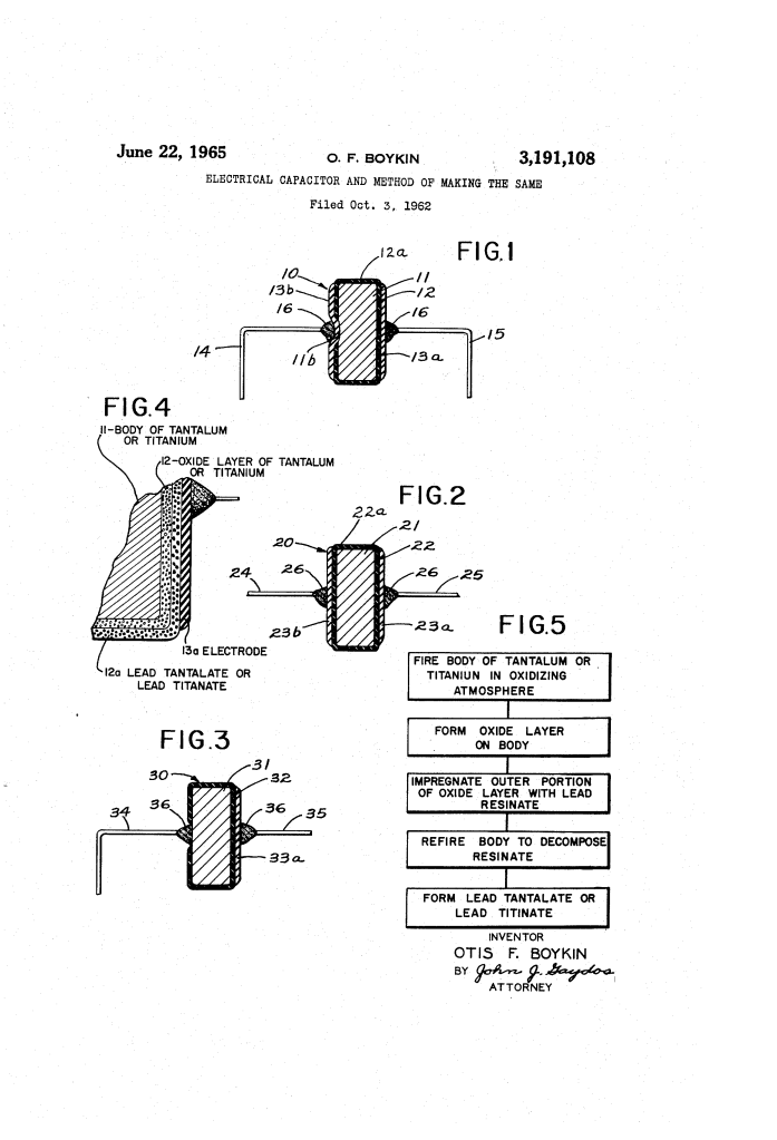
- Controlled Base Metallurgical Oxidation: A solid, high-purity cylindrical body composed of a refractory metal (either tantalum or titanium) is thermally treated in an oxidizing atmosphere within a kiln at temperatures ranging from 700^C to 900^C for a duration of 5 to 30 minutes. This initial calcination synthesizes a high-retentivity native metal oxide layer (titanium dioxide or tantalum pentoxide) cleanly bonded to the unoxidized conductive core.
- Metallo-Organic Chemical Interdiffusion: The outer boundary of this newly formed native oxide layer is subsequently impregnated via submersion in a liquid lead resinate solution. Upon refiring the body at 800^C for approximately 5 to 10 minutes, the lead resinate thermally decomposes. This triggers a solid-state localized reaction where the active lead ions chemically bind with the upper sub-layers of the native oxide.
- Adhesive Phase Transition Maintenance: Crucially, this reaction is halted before it can penetrate the entire depth of the native oxide layer. By leaving a clean, unreacted layer of native oxide contiguous to the core metal body, the structural atomic bond between the metal electrode and the ceramic dielectric is preserved, preventing the dielectric from breaking or brushing away from the core. The resulting multi-phase dielectric film manifests a high dielectric constant with consistently reproducible electrical traits.
Differential Substrate Termination Assembly
- Localized Mechanical Stratum Removal: To transform the core metallurgical pellet into an active primary capacitor electrode, the synthesized dielectric film must be breached. One parallel end of the treated cylinder is subjected to a precise sandblasting or grinding process. This cleanly shears away the ceramic dielectric coating to expose a distinct section of the underlying unoxidized metal substrate.
- Screened Screen-Printed Electrode Deposition: A conductive silver paste formulation is screened directly over the sandblasted section of the core, while a separate layer of conductive silver paste is applied to the intact ceramic compound coating the opposite end of the pellet.
- Vitrified Fused Terminal Attachment: The entire component is fired a final time to vitrify and fuse the glass frits within the silver paste directly to the targeted surfaces. This creates two isolated termination blocks: one connected to the inner core electrode and the other bonded to the outer dielectric face. Electrical lead wires are then anchored to these silver deposits via mechanical solder reflow or deposition.
Integrated Symmetrical Pre-Oxidation Lead Anchor
- Pre-Thermal Structural Welding: In an alternate configuration designed to fully bypass the mechanical abrading or sandblasting phase, a primary electrical lead wire is directly welded or soldered via a metal deposit to the raw titanium or tantalum body prior to any chemical conversion steps.
- Co-Processed Thermal Passivation: The combined lead-and-body assembly is then routed into the oxidizing kiln. As the native oxide film and the subsequent lead-infused ceramic dielectric compounds are grown around the rest of the body, a secure electrical junction remains intact beneath the dielectric layer.
- Ablation-Free Structural Termination: An external secondary silver electrode paste is then applied over the opposite surface of the freshly grown dielectric layer and fired. This configuration provides a complete circuit connection to both the internal and external zones of the dot capacitor without requiring any post-chemical abrasive processing.
Comparison Table
| Technical Metric / Feature | Standard Methods of the Time (Independent Dielectric Assembly) | The New Innovation (Boykin In-Situ Perovskite Capacitor) |
| Dielectric Layer Architecture | Separately formed ceramic or mica sheets mechanically bonded to metal plates. | Symmetrically grown, multi-phase native oxide and lead-compound ceramic dielectric. |
| Volumetric Capacitance Density | Low; large physical volume required to achieve high capacitance values. | High capacity-to-volume ratio (“dot capacitor” layout optimized for compact packaging). |
| Thermal Deflection Stability | High drift; capacitive values altered significantly across wide temperature swings. | Minimal drift; displays a flat variation coefficient of approximately 2 from 15^C to 85^C. |
| Interfacial Delamination Risk | High; distinct adhesive bounds are prone to structural shearing under thermal or mechanical stress. | Eliminated; gradient metallurgical transition maintains an atomic bond between core and dielectric. |
| Manufacturing Yield and Precision | Inconsistent electrical profiles due to air entrapment and varying paste thickness. | Consistently reproducible electrical parameters governed by regulated kiln cycles and liquid resinate dips. |
Significance Section
- Pioneered Modern Surface-Mount Technology (SMT): The geometry and chemical layout of Boykin’s dot capacitor directly anticipated the sub-miniature, leadless multi-layer ceramic capacitors (MLCCs) that form the baseline of modern high-density surface-mount circuit boards.
- Precursor to High-K Dielectric Semiconductor Processing: The concept of converting a native metal surface into an oxide layer and then doping it with heavy metal ions to boost the dielectric breakdown constant serves as an early mechanical analog to modern atomic layer deposition (ALD) methods used to build high-k metal gates in contemporary microprocessors.
- Foundational Concept for Thin-Film Hybrid Modules: Boykin’s work optimizing components specifically for “Swiss Cheese” or breadboard packaging frameworks laid the groundwork for the micro-module and multi-chip module (MCM) integration technologies later adopted by aerospace and deep-space computational hardware platforms.
Next Step
To further analyze the system’s electrical performance, the next step is to evaluate the Dielectric Interface Permittivity across the multi-phase boundary. By calculating the total capacitance of the dual-layer configuration using the series capacitance relation:
1/C_total= 1/C_oxide + 1/C_titanate = d_1/kappa_1 epsilon_0 A + d_2/kappa_2 epsilon_0 A
where d_1 and d_2 represent the localized thicknesses of the unreacted native oxide and the lead-reacted titanate/tantalate layers respectively, and kappa_1 and kappa_2 define their specific dielectric constants, engineers can model the optimal chemical diffusion depth. This calculation will maximize the component’s total capacity while ensuring the unreacted native oxide backing layer remains thick enough to prevent structural delamination from the core substrate.
