
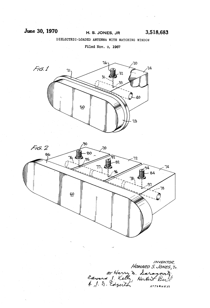
Dielectric-Loaded Antenna with Matching Window (1970)
U.S. Patent No. 3,518,683, granted on June 30, 1970, to Howard S. Jones, Jr., addresses a critical engineering bottleneck in aerospace and defense communications: the excessive weight, bulk, and thermal vulnerability of microwave waveguide antennas aboard atmospheric re-entry vehicles, missiles, and spacecraft.
Standard microwave systems relied on thick-walled brass or copper alloy waveguides that were heavy, cumbersome, and expensive. Furthermore, transmitting radar or communication signals through the outer hull of a re-entry vehicle required installing a separate, heat-resistant window adjacent to the metal antenna. Jones, an inventor based in Washington, D.C., working for the U.S. Army, eliminated the heavy metal tubing and separate window entirely by carving the entire antenna and its exterior radiating window out of a single monolithic block of heat-resistant dielectric material.
The Innovation: The Monolithic Dielectric Structure
Standard hollow waveguides require substantial volume to propagate microwaves. Jones utilized the physical principle of dielectric loading: filling the waveguide with a dense dielectric medium scales down the physical dimensions by a factor inversely proportional to the square root of the dielectric constant (E).
Instead of packing a metal tube with ceramic, Jones inverted the manufacturing paradigm:
- Shaping the Core: A single block of high-temperature dielectric material (such as fused silica, aluminum oxide, or boron nitride) is machined to match both the internal dimensions of the waveguide and an integrated radiating window (23) at the front.
- Conductive Plating: Rather than housing the dielectric inside heavy metal walls, a thin, highly conductive metallic film is plated directly onto the exterior surfaces of the shaped dielectric block (24). This plated layer is engineered to be just thick enough to carry radio frequency (RF) currents.
- The Integrated Window: The front radiating face (50) of the dielectric block is intentionally left unplated. This unplated surface acts as the antenna window, mounting flush with the exterior skin or heat shield of the spacecraft.
Key Technical Advantages
The design delivers three decisive advantages for high-performance aerospace systems:
Weight and Bulk Reduction: Replaces heavy copper and brass alloy walls (typically 0.025 to 0.125 inches thick) with a microscopic conductive plated film, slashing total payload weight. Direct Heat-Shield Integration: Using refractories capable of withstanding 500 to 4,000 degrees Fahrenheit allows the window to sit directly in the vehicle’s thermal protection shield without requiring separate seals or secondary outer windows. Beam Steering and High Gain: By fabricating multiple parallel cavities (70, 72, 74) out of the same monolithic block feeding into a single common window (86), the antenna can control radiation angles and boost signal gain via phase control across the cavities.
System Components and Mechanics
| Component | Description | Function |
| Dielectric Core (24) | Solid fused silica, aluminum oxide, or boron nitride | Reduces waveguide cross-section via dielectric loading while withstanding severe re-entry temperatures. |
| Conductive Coating | Thin metallic plating across waveguide walls | Replaces heavy structural tubing, guiding RF current with minimal weight. |
| Radiating Window (23, 50) | Unplated monolithic extension of the dielectric core | Transmits electromagnetic energy out of the vehicle flush with the heat shield. |
| Mounting Flange (21) | Perimeter flange encircling the window | Secures the monolithic antenna flush to the spacecraft hull. |
| T-Bar Feed (26, 31, 40) | Coaxial connector with center pin soldered inside transverse plated bore | Feeds RF energy directly into the dielectric waveguide cavity. |
How the Single and Multi-Cavity Systems Function
- Signal Input: High-frequency RF energy enters through a coaxial connector (26). The outer conductor grounds to the metallic plating at point 32, while the center conductor (31) couples to a transverse plated hole (40) drilled through the dielectric core.
- Wave Propagation: The signal propagates through the miniaturized dielectric section, guided by the plated metallic skin.
- Direct Radiation: As the wave reaches the unplated front face (50), it radiates outward into space without encountering an air gap, boundary reflection, or secondary protective pane.
- Multi-Cavity Array Operation: In the multi-cavity configuration (FIG. 2), three cavities (70, 72, 74) share a single continuous dielectric window (86/60). By adjusting the signal phase feeding connectors 80, 82, and 84, operators can electronically steer the radiating beam off-axis and achieve higher gain than a single cavity allows.
Historical and Scientific Impact
Granted under Title 35 to the Secretary of the Army, Jones’s invention solved one of the toughest packaging constraints of the Space Race and Cold War missile development: maintaining reliable communications during atmospheric entry.
Aerospace Miniaturization: Proved that structural waveguide walls could be eliminated in favor of plated dielectric substrates, laying early groundwork for conformal and flush-mounted aerospace antennas. Thermal Survivability: Enabled flush-mounted antenna arrays that could survive the extreme plasma and heating environments of re-entry without compromising aerodynamic contours. Manufacturing Economy: Replaced complex multi-part brazed assemblies with a single machined, plated ceramic block, significantly reducing fabrication failure rates.
About the Inventor: Howard S. Jones, Jr.
Howard S. Jones, Jr. was an acclaimed African American physicist, engineer, and inventor who served for decades at the Harry Diamond Laboratories (HDL) in Washington, D.C.
Patents and Innovations: Jones held over 30 patents in microwave circuits, radomes, and conformal antenna arrays, authoring seminal papers on spacecraft antenna miniaturization and dielectric-loaded waveguides. Pioneering Impact: His designs for flush-mounted and conformal antennas became standard fixtures across advanced rocketry, artillery proximity fuzes, satellite platforms, and missile defense systems. Legacy: Jones was inducted into the National Academy of Engineering and elected a Fellow of the Institute of Electrical and Electronics Engineers (IEEE), recognized as one of the preeminent microwave antenna designers of the modern era.
Summary of Claims
The patent explicitly claims:
- A microwave antenna constructed from a solid mass of high-temperature dielectric material shaped to standard waveguide dimensions, featuring an integral, enlarged radiating window.
- A thin metallic coating covering the dielectric body to carry RF currents while leaving the radiating window uncoated.
- The use of refractory dielectrics specifically chosen from fused silica, aluminum oxide, and boron nitride.
- A multi-cavity monolithic embodiment comprising several waveguide channels feeding into a single, contiguous dielectric window for directional radiation and enhanced gain.
